
As Moore’s Law becomes harder and harder to sustain, the semiconductor industry is looking for new ways to improve communication speeds, use less chip real-estate and reduce power consumption. Using optical glass as an interconnect material addresses many of these concerns and opens the door to new architectures with increased complexity compared to what is available historically.
When writing optical waveguides in transparent materials, due consideration must be given to dispersion and aberrations introduced by the material. This problem becomes much more complex when true 3-dimensional structures are required.
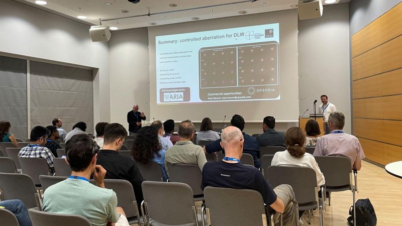
Opsydia have solved these problems by developing an adaptive optic direct laser writing system based on the groundbreaking work of our founding scientists, Prof. Martin Booth and Prof. Patrick Salter at the University of Oxford
The Opsydia P5000 photonics system is designed specifically for the challenging world of optical interconnects.
Overcomes material induced optical aberrations
Improved feature size & elimination of material damage
Precisely locates intended waveguide origin and termination
Ensures higher yield and lower alignment costs
High uptime, remote diagnostics, true 24/7 operation
Easy to optimise recipe. Batch Mode for higher volumes